Journal of Physics: Materials
Contact transparency in mechanically assembled 2D material devices
Journal of Physics: Materials · 2, 035003 (2019)
Read original paper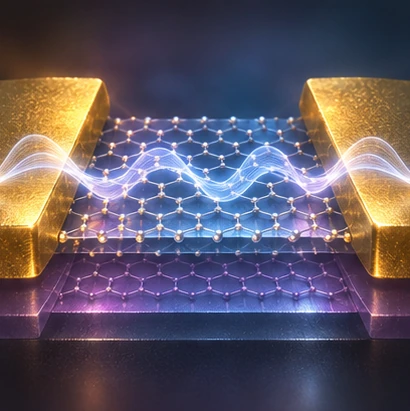
Introduction
Two-dimensional crystals are mechanically transferred onto contacts to form junctions with superconductors. Transport measurements indicate comparable or better interface transparency than in conventionally patterned devices, with contact roughness a prominent limitation.
A closer reading
Preparing the contacts separately reduces processing of the more fragile crystal. The comparison also makes clear that avoiding processing damage is only part of the problem: roughness at the surface can still limit electronic transmission.